🚀 2D Transistors Are Coming Faster Than Expected! MIT Startup May Cut Timeline in Half
✨ Key Highlights for Exam & Quick Reading
- MIT spinout CDimension may cut the 10-year wait for 2D transistors down to 5 years.
- They developed a low-temperature process to grow MoS₂ (a 2D semiconductor) directly on silicon.
- This innovation could lead to ultra-powerful, energy-efficient 3D chips.
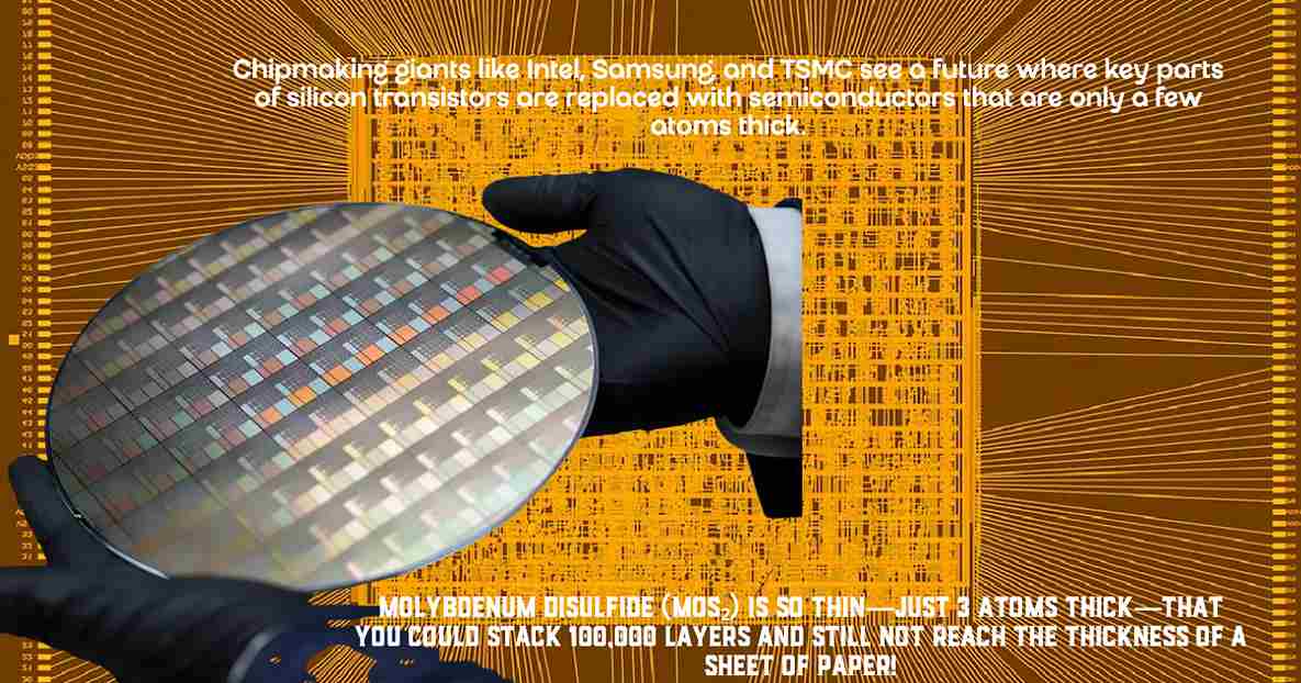
- Could replace traditional silicon in the tiniest parts of future chips.
- Consumes 1/1000th the power of current silicon devices.
🧠 What’s the News?
A revolutionary breakthrough by a startup from MIT—CDimension—could bring futuristic 2D transistors to your smartphones, laptops, and other electronics sooner than expected. They’ve developed a way to grow super-thin semiconductors directly onto silicon chips—something previously thought to be a decade away.
🔍 What Did They Find & Why It Matters?
💡 The Big Idea
Today’s chips rely on silicon transistors—tiny switches that power your devices. But as chips get smaller and faster, silicon is reaching its physical limits. Scientists worldwide are searching for alternatives.
Enter 2D semiconductors—materials that are just a few atoms thick!
CDimension’s innovation lies in using a low-temperature process (200°C) to grow molybdenum disulfide (MoS₂) directly on silicon. This solves a major problem—normally, growing such materials requires temperatures over 1000°C, which would damage the chip.
This opens the door to layering 2D materials on top of current silicon chips, leading to 3D chips with better performance and less power usage.
🧪 A Simple Way to Understand It
Imagine you want to add a second floor to a house made of jelly (fragile silicon). Normally, building on top would melt the house! But CDimension found a way to gently add that second floor without melting the base. That’s how game-changing their low-temp growth technique is.
🗣️ What the Researchers Say
“Most people still think of 2D semiconductors as lab-only materials,” says Jiadi Zhu, CEO and co-founder of CDimension. “But we’ve solved big problems like making uniform 2D layers, ensuring good performance, and making it work with existing chip-making tech.”
🔧 What Else Did They Do?
CDimension is already shipping silicon wafers with 2D materials for chipmakers like Intel, Samsung, and TSMC to test. These materials don’t just save energy—they may allow devices to run on half the voltage.
In fact, their tests show that MoS₂ transistors can use 1/1000th the energy of today’s silicon ones!
They’re also working with tungsten diselenide (p-type) and hexagonal boron nitride (insulator) to complete the puzzle for future CMOS (logic) chips.
🔍 Why It Matters
- ⚡ Power Saver: 2D transistors use less energy, making future devices faster and cooler.
- 📏 Super Small: These atom-thin layers are perfect for building ultra-compact chips.
- 🧠 Smarter Tech: They could revolutionize AI processors, smartphones, and even space electronics.
- 🔁 Compatible: It works with today’s chipmaking machines, so adoption could be quick.
❓ Quick Quiz – Test Yourself!
- What material does CDimension use to build 2D transistors?
A. Graphene
B. MoS₂
C. Silicon
D. Copper
✅ Correct: B. MoS₂ (Molybdenum Disulfide) - Why is the 200°C growth process special?
A. It’s faster
B. It reduces chip cost
C. It prevents damage to silicon
D. It makes the chip bigger
✅ Correct: C. It prevents damage to silicon - Which chipmakers are exploring 2D semiconductors?
A. Google, Apple, Meta
B. Intel, Samsung, TSMC
C. AMD, NVIDIA, Tesla
D. None of the above
✅ Correct: B. Intel, Samsung, TSMC - What’s the expected timeline now for 2D chip integration?
A. 2 years
B. 5 years
C. 10 years
D. 15 years
✅ Correct: B. 5 years
🤯 Fun Science Fact
Molybdenum disulfide (MoS₂) is so thin—just 3 atoms thick—that you could stack 100,000 layers and still not reach the thickness of a sheet of paper!